

有关: 光子学
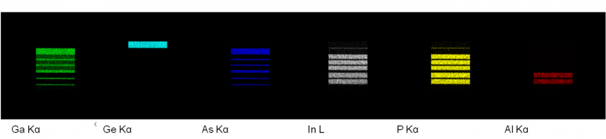
Ensuring optimal emission from any device requires high-quality fabrication. From uniform quantum well depth in GaAs/AlGaAs to smooth sidewalls in InP waveguides or GaN high brightness LEDs we have the process solution. Our long experience in the processing on GaN and III-V materials means that we understand what it takes to deliver high throughput of high-quality devices in batch or single wafer fabrication. Our GaN etch is low damage to maintain surface quality while we offer both selective and non-selective etches for GaAs/AlGaAs to provide optimum quality whether the challenge is no notching of side walls in VCSELs or accurate depth control. Once a process has been completed it is very obviously important to characterise the results. Photonic multiple quantum well structures can have QW depths of less than 5 nm. For these structures, elemental characterisation is usually achieved using elemental dispersive spectroscopy and transmission electron microscopy (TEM). Our range of X-Max EDS detectors for TEM ensures high throughput and accurate results due to optimised sensors that deliver the highest possible sensitivity. This allows the mapping of nanometer size device features in minutes so that the real distribution of elements in a specimen can be characterised and the success of a fabrication process understood.
Process solutions for GaAs AlGaAs
Process solutions for InP InGaAs InAlAs
Process Solutions for HBLED Applications
© 牛津仪器 2026
 公安机关备案号31010402003473